


FR4 - High Thermal Conductivity (HTC) Laminates -FR4 HTG - Halogen Free Laminates - Panasonic Megtron6 - ISOLA Astra MT - Nelco - Rogers - Polyamide - Ventec
Back Panel
Back Panel (Wafer Probe Card)
In today's High Tech society, semiconductor integrated circuits are essential. They can be found within a wide range of products, from simple calculators to the fastest computers, and as a result the production of printed circuit boards back panel (wafer probe cards) has become a hugely important industry involving some of the world's most advanced technologies.
The back panel circuits are important in the final stage of this manufacturing process by playing a key role in the analysis and measurement of integrated printed circuit boards.
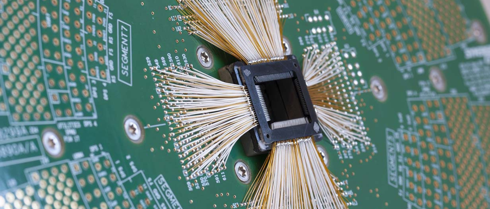
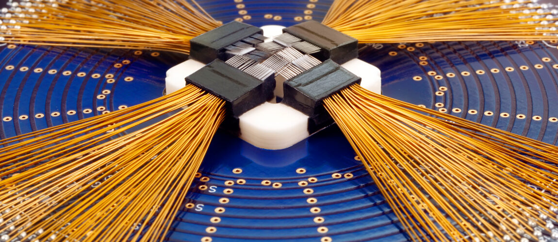
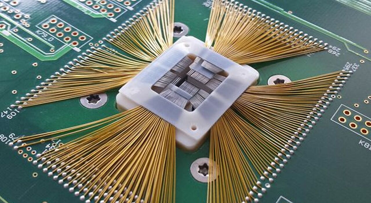
BACK PANEL (WAFER PROBE CARD)
In today's High Tech society, semiconductor integrated circuits are essential. They can be found within a wide range of products, from simple calculators to the fastest computers, and as a result the production of printed circuit boards back panel (wafer probe cards) has become a major industry involving some of the most advanced technology in the world. Back-panel circuits are important in the final stage of this production process, playing a key role in the analysis and measurement of integrated circuit boards.
The Back Panel Circuit (Probe card) are built with Multilayers technology. Usually these PCBs are very complex, as they feature very high number of Layers (Up to 80layers). In addition to this important aspect, the probe card have other critical issues such as : Final thickness of the PCB very high (8/10mm), Very gentle drilling (Press-fit), Mixed surface finishes very critical (ENIG + Hard Gold), stringent impedance controls, and delicate mechanical finishes such as Flaring/Beveling and other special machining.

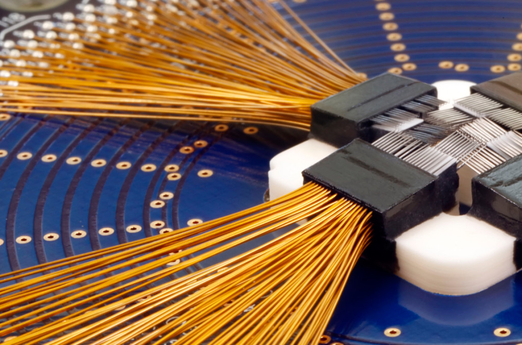
The Back Panel Circuit (Probe cards) are built with Multilayers technology. Usually these PCB are very complex, as they are characterised by a very high number of layers (up to 80 layers). In addition to this important aspect, probe cards present other critical aspects such as: very high final PCB thickness (8/10mm), very delicate drillings (Press-fit), Mixed surface finishes very critical (ENIG + Hard Gold), stringent impedance controls, and delicate mechanical finishes such as Flaring/Beveling and other special machining.
80
610 x 780 mm
Standard: 0.085 mm
Custom: 0.050 mm
Standard: +/- 10 %
Custom: +/- 5 %
18-35-70 um
Passivated Copper ( OSP ) - Hot Air Levelling Lead Free HAL or Sn/Pb - Chemical Gilding ( ENIG- ENIPIG-ASIG ) - Electrolytic Gilding - Chemical Silver - Chemical Tin
Green-blue-red-white-black and transparent. Some colors are also available in matte and glossy versions
White, black, blue, yellow, red
- Single printed circuit board
- Printed circuit board in Panel
- Printed circuit board in quadrotto with witnesses
- Panel with pre-cuts V-Scoring
- Mixed Technology (Milling and V-Scoring)
- Height-controlled machining
- Beveling, Countersinking, Reaming
Back Panel
Back Panel
Back Panel
Back Panel
APPLICATION MARKETS
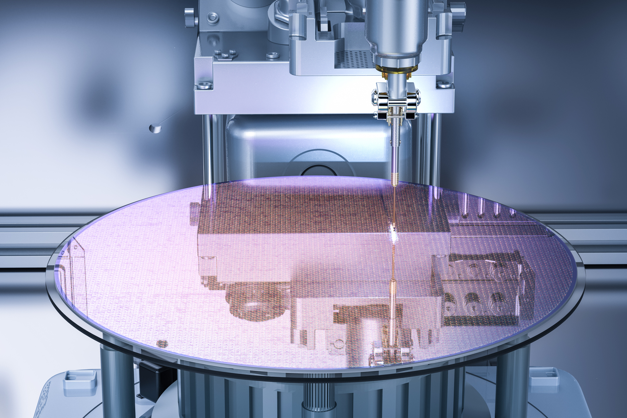
Semiconductor Manufacturing |
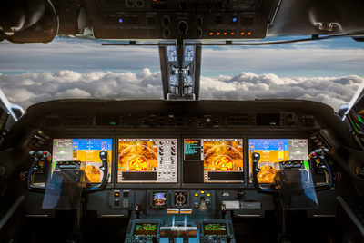
Aeronautical |
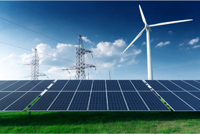
Energy |